
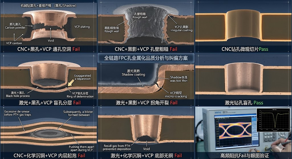
Comprehensive Analysis of All Failure Paths in 6-Hole FPC Metallization Processes and High-End Selection Guide
In modern high-density multilayerflexible PCB(flexible circuit board) andflexible PCBAIn the manufacturing of (flexible printed circuit assemblies), the processing and metallization of micro-vias are absolutely critical to the reliability of the overall electrical interconnects. Whenflexible PCBADuring high-temperature reflow, thermal shock, or high-frequency/high-speed signal transmission, even microscopic copper voids, delamination, or cracks can become catastrophic "signal black holes."
Different hole-making methods (mechanical drilling vs. laser drilling) combined with various metallization techniques (black oxide, black image, and electroless copper plating) have given rise to 6 mainstream process families, each with its own strengths and limitations. To help hardware engineers and procurement experts worldwide make efficient selections and avoid impedance discontinuities and via failures during mass production, our technical team has conducted a comprehensive multi-dimensional analysis of the advantages and disadvantages across these 6 technology routes:
I. Direct Conductive Technology: The "Black Hole" Approach (Carbon Black Process)
Black hole plating deposits fine carbon particles onto the inner walls of holes to form a conductive layer, offering a highly cost-effective direct electroplating solution.
Route 1: CNC drilling + black hole + VCP
Craftsmanship AnalysisAfter mechanical drilling, the holes are cleaned and lightly etched to physically adsorb fine carbon particles onto the non-conductive hole walls. The boards then proceed directly to a Vertical Continuous Plating (VCP) line for copper buildup.
Advantages: Highly competitive cost, streamlined process flow, and simplified wastewater treatment. The micro-roughness of the hole walls created by mechanical drilling facilitates strong physical adhesion of carbon powder particles. In through-holes with low to medium densityflexible PCBExtremely high production efficiency.
disadvantageNot suitable for small-diameter holes (less than 0.2 mm). Mechanical drilling can cause burrs and resin smear. If desmear is incomplete, carbon residue tends to adhere unevenly at the hole walls. Under high current during VCP, microscopic current concentrates locally on rough surfaces, which may ultimately lead toLocalized thin copper plating in holes or voids in through-holes。
Route 2: Laser Drilling + Black Hole + VCP
Craftsmanship AnalysisUtilize UV or CO₂ laser to drill blind holes in HDI structures, then use black hole lines to allow carbon powder suspension to penetrate the bottom of the blind holes, forming a conductive precursor for subsequent electroplating.
Advantages: Bare-board processing costs are significantly lower than traditional electroless copper plating, with shorter cycle times—ideal for cost optimization in consumer electronics.
disadvantage: Laser ablation generates intense heat, leaving stubborn carbonized layers and residues at the bottom of blind vias. Due to the relatively large particle size of black hole carbon powder, wettability and flow resistance are poor at the bottom of micro blind vias with high aspect ratios. After electroplating, voids are highly likely to form at the via bottom.Subtle "delamination" or incomplete via filling。
II. Direct Conductive Technology: The "Shadow" School (Graphite Shadow Process)
The Shadow Black process uses a finer graphite colloid than toner, creating a thinner conductive layer that offers enhanced penetration into micro-pores after modification.
Route 3: CNC Drilling + Blackout + VCP
Craftsmanship AnalysisAfter mechanical drilling, a selective graphite adsorption process using black shadow lines creates an atomically thin graphite conductive film on the hole wall, followed by VCP electroplating.
AdvantagesGraphite particles are extremely fine, providing significantly more uniform coverage on mechanical hole walls than black holes and resulting in lower copper layer stress after electroplating. Completely eliminates formaldehyde from traditional PTH processes for a green, eco-friendly solution.
disadvantage: Requires extremely tight process windows for pretreatment (via drilling). If drill bit wear causes uneven roughness on the mechanical hole walls, tiny air bubbles can easily become trapped during shadow dye immersion. Under the high-velocity fluid冲击 in VCP plating, unshadowed areas will fail to conduct, directly causingCopper Plating Delamination and Voiding at Hole Centers。
Route 4: Laser Drilling + Shadowing + VCP
Craftsmanship AnalysisFor high-density micro-vias, leverage the excellent dispersion of graphite colloid to penetrate into laser-drilled micro-vias and establish electroplating pathways.
AdvantagesA cost-effective balance for high-density micro-vias. Fine graphite particles wet laser-drilled via sidewalls smoothly, and when combined with the efficient mass transfer of VCP plating, they deliver excellent via filling performance.
disadvantage: Due to the inherent taper of laser-drilled micro-vias, graphite layers tend to thin at corner regions where black ink flows through, caused by flow resistance. Under high-temperature thermal shock during reflow soldering or prolonged dynamic bending,Micro-cracking is likely at blind hole corners due to stress concentration.。
3. Classic Reliability: Electroless Copper / PTH
Traditional chemical self-catalytic copper deposition forms a continuous, atomically thin layer of metallic copper on孔 walls, serving as the foundation for advanced manufacturing.
Route 5: CNC Drilling + Chemical Copper Plating + VCP
Craftsmanship AnalysisAfter mechanical drilling, the desmearing process is strictly applied. A palladium catalyst initiates a chemical redox reaction on the non-conductive surfaces of the hole walls to deposit a continuous, seamless thin copper layer, followed by VCP thickening.
AdvantagesThrough chemical etching and autocatalytic reactions, the electroless copper layer achieves an unparalleled mechanical interlocking effect with the hole walls, delivering superior bond strength. The resulting through-hole plating is exceptionally full and robust.
disadvantageThe process is lengthy with numerous monitoring points for chemicals, requires large equipment footprint, and incurs high waste liquid treatment costs. Excessive etching in the pre-process can cause over-cellularization of the PI substrate, leading to trapped micro-bubbles between layers that may result in blistering and delamination during high-temperature assembly.
Route 6: Laser Drilling + Chemical Copper Deposition + VCP
Craftsmanship AnalysisAfter high-precision laser drilling of microvias, a seamless pure copper layer is deposited on the inner walls and bottom pads via electroless copper plating, followed by perfect via fill using VCP.
Advantages:The absolute first choice for automotive-grade, high-end medical, and high-frequency/high-speed FPCs!Chemical copper plating delivers an atomically continuous, fully covered conductive layer with zero dead zones—regardless of how small the blind hole diameter or how extreme the aspect ratio. Tight grain bonding at the blind hole bottom eliminates delamination and cracking risks entirely, maximizing dynamic flex life.
disadvantage: Has the highest comprehensive manufacturing cost and involves the most complex processes. In extremely small blind holes, if hydrogen byproducts from electroless copper plating cannot be vented, it requires exceptionally high-precision horizontal or vertical vibration control systems, demanding deep equipment expertise from the manufacturer.
6 Process Combination: Multi-Dimensional Performance Dashboard
Process Route Combination | blind hole coverage | Dynamic Bending Life | Signal Integrity (SI) | Total Manufacturing Cost | Core Application Areas |
1. CNC + Black Hole + VCP | Poor | Standard | Standard | Very Low | Consumer Single/Dual-Layer and Standard Multi-Layer Boards |
2. Laser + Black Hole + VCP | Medium | Medium | Standard | Lower | Cost-effective smart hardware, backlit panels |
3. CNC + Shadow + VCP | Medium | Good | Good | Medium | Eco-friendly smart wearables and consumer-grade network cards |
4. Laser + Shadow + VCP | Good | Good | Good | Medium | Connect mid-to-high-end smartphones and tablets |
5. CNC + Chemical Copper Plating + VCP | Uniqlo | Uniqlo | Uniqlo | High | Multi-layer rigid-flex boards, industrial control equipment |
6. Laser + Chemical Copper Deposition + VCP | Excellence | Excellence | Excellence | High | Automotive Instrument Clusters / ADAS, Medical Endoscopes, Thunderbolt/USB4 High-Speed Cables |
4. Why Choose Us? Overcoming the "Impedance and Yield" Challenge with Precision Engineering
at the high endflexible PCBAIn our supply chain, we are more than just a manufacturer; we are your Signal Integrity (SI) assurance expert. To meet the rigorous demands of high-frequency, high-speed, and high-reliability products, we have closed-loop upgraded the aforementioned processes:
Strict Microscopic Cross-Section Plating Sequence ControlAcross all VCP and surface treatment lines, we strictly enforce a cross-sectional sequence: micro-via copper electroplating followed by precision surface protective layers (e.g., tin/gold). The initial pure copper plating ensures perfect lattice integration on hole walls and blind via bottoms, while the subsequent precision protection layer provides an optimal oxidation barrier, completely eliminating signal dispersion caused by the skin effect under high-frequency current.
Impedance-integrated design based on Polar Si9000eRegardless of the via metallization combination you choose, we parameterize via sidewall trapezoidal tolerance, resin flow deformation, and layer stack-up thickness into our simulation models to precisely control high-speed differential impedance within a ±5% golden tolerance.
Enterprise Hardware Benchmark Calibration Verification: We are equipped with such asE5071C Vector Network AnalyzerandAgilent 86100D High-Speed OscilloscopeBenchmark industry testing matrices. Before delivery, every batch of high-speed/multi-layer FPC must undergo rigorous time-domain reflectometry (TDR) impedance continuity scans, real-time jitter analysis, and high-speed eye diagram testing to ensure compliance with hard threshold requirements for high-speed protocols such as USB 3.0 and Thunderbolt.
Whether your project demands ultimate cost-efficiency or maximum reliability in extreme environments, we deliver the most scientifically optimized process combinations and micrometer-level metallographic analysis to build a rock-solid "flexible tech skeleton" for your hardware innovation.